M93C66-RMN6TP 查看數據表(PDF) - STMicroelectronics
零件编号
产品描述 (功能)
生产厂家
M93C66-RMN6TP
STMicroelectronics
M93C66-RMN6TP Datasheet PDF : 37 Pages
| |||
M93C86, M93C76, M93C66, M93C56, M93C46
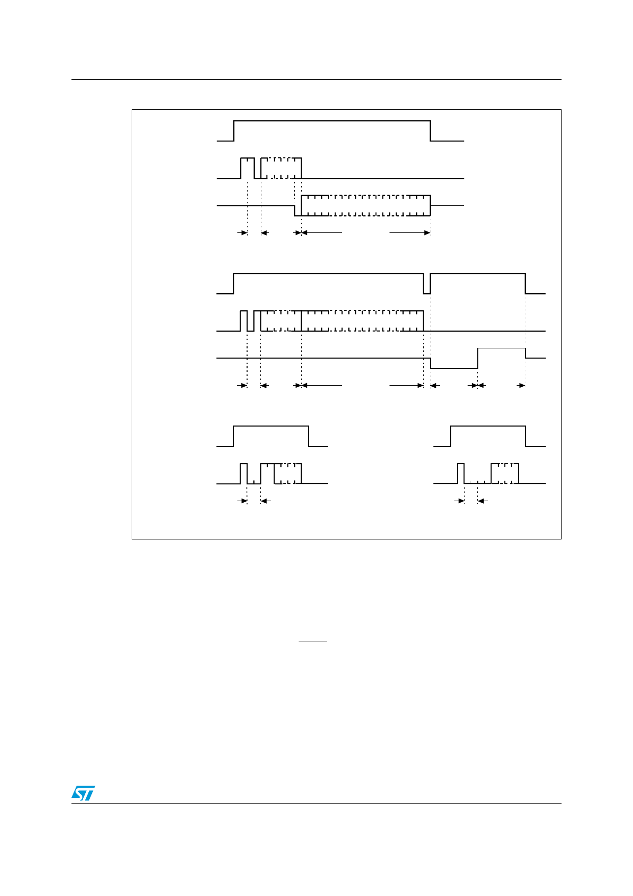
Figure 4. READ, WRITE, WEN, WDS sequences
Read
S
Instructions
D
1 1 0 An A0
Q
Write
S
D
Qn
Q0
ADDR
OP
CODE
DATA OUT
1 0 1 An A0 Dn
CHECK
STATUS
D0
Q
Write
S
Enable
D
ADDR
OP
CODE
1 0 0 1 1 Xn X0
DATA IN
BUSY
READY
Write
S
Disable
D
1 0 0 0 0 Xn X0
5.3
OP
CODE
1. For the meanings of An, Xn, Qn and Dn, see Table 5., Table 6. and Table 7..
OP
CODE
AI00878d
Erase Byte or Word
The Erase Byte or Word (ERASE) instruction sets the bits of the addressed memory byte (or
word) to 1. Once the address has been correctly decoded, the falling edge of the Chip
Select Input (S) starts the self-timed Erase cycle. The completion of the cycle can be
detected by monitoring the READY/BUSY line, as described in the READY/BUSY status
section.
15/37
Share Link: 