M25P05-AVMP6TP 查看數據表(PDF) - Numonyx -> Micron
零件编号
产品描述 (功能)
生产厂家
M25P05-AVMP6TP Datasheet PDF : 52 Pages
| |||
Initial delivery state
M25P05-A
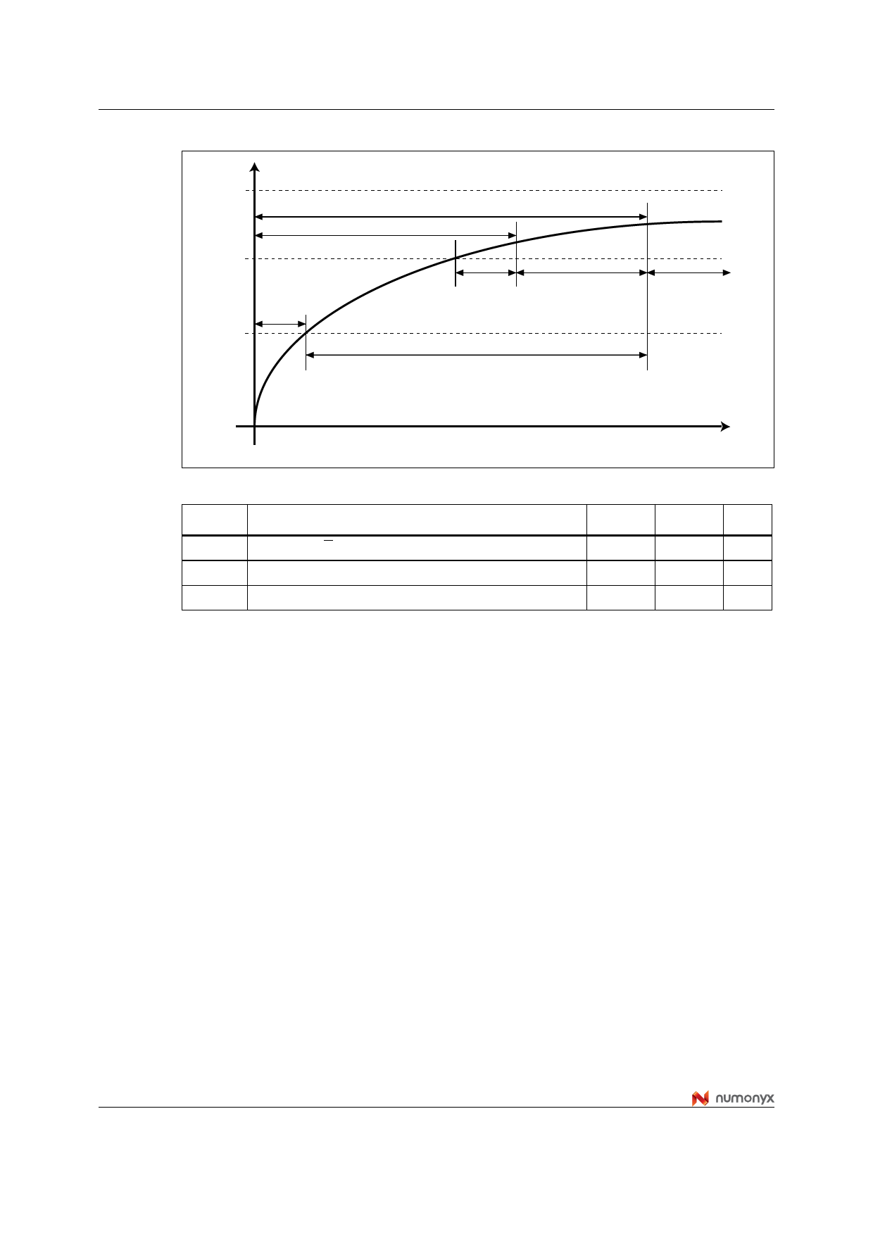
Figure 20. Power-up timing
VCC
VCC(max)
Program, erase and write commands are rejected by the device
Chip selection not allowed
VCC(min)
VWI
Reset state
of the
device
tVSL
Read access allowed
tPUW
Device fully
accessible
Table 8.
Symbol
Power-up timing and VWI threshold
Parameter
tVSL(1)
tPUW(1)
VWI(1)
VCC(min) to S low
Time delay to Write instruction
Write inhibit voltage
1. These parameters are characterized only.
time
AI04009C
Min
Max Unit
10
µs
1
10
ms
1
2
V
8
Initial delivery state
The device is delivered with the memory array erased: all bits are set to ‘1’ (each byte
contains FFh). The status register contains 00h (all status register bits are 0).
36/52
Share Link: 