STM32F302VB View Datasheet(PDF) - STMicroelectronics
Part Name
Description
MFG CO.
STM32F302VB Datasheet PDF : 133 Pages
| |||
Electrical characteristics
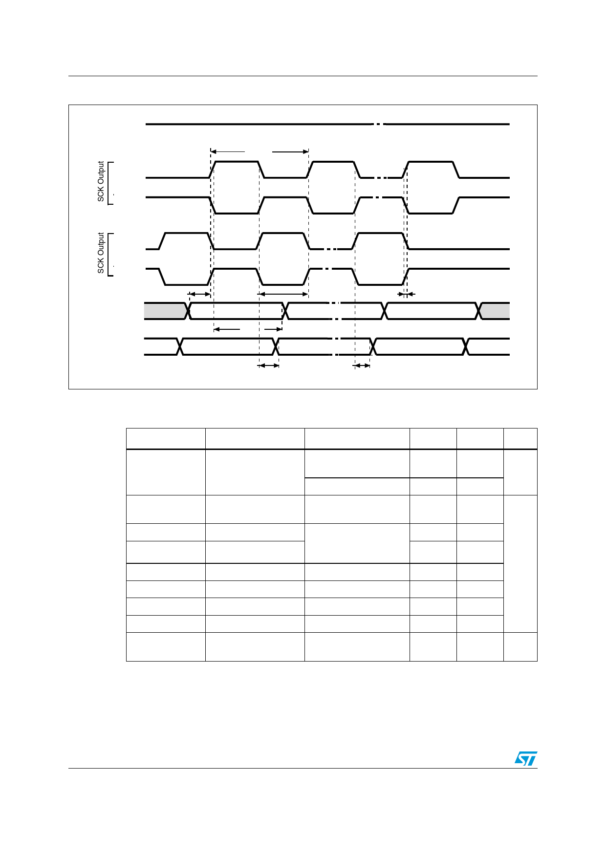
Figure 28. SPI timing diagram - master mode(1)
(IGH
.33�INPUT
#0(!
#0/,
#0(!
#0/,
TC3#+
STM32F302xx/STM32F303xx
#0(!
#0/,
#0(!
#0/,
-)3/
).0 54
TSU-)
-/3)
/5405 4
TW3#+(
TW3#+,
-3 ").
TH-)
- 3"�/54
TV-/
") 4�).
" ) 4�/54
TH-/
TR3#+
TF3#+
,3"�).
,3"�/54
AI6
1. Measurement points are done at 0.5VDD and with external CL = 30 pF.
Table 62. I2S characteristics
Symbol
Parameter
Conditions
Min
Max Unit
fCK
1/tc(CK)(1)
tr(CK)
tf(CK)(1)
tw(CKH) (1)
tw(CKL) (1)
tv(WS) (1)
th(WS) (1)
tsu(WS) (1)
th(WS) (1)
Duty Cycle(1)
I2S clock frequency
I2S clock rise and fall
time
I2S clock high time
I2S clock low time
WS valid time
WS hold time
WS setup time
WS hold time
I2S slave input clock
duty cycle
Master data: 16 bits,
audio freq=48 kHz
Slave
Capacitive load
CL = 30 pF
Master fPCLK= 36 MHz,
audio frequency =
48 kHz
Master mode
Master mode
Slave mode
Slave mode
Slave mode
1.496
0
-
331
332
4
4
4
0
30
1.503
12.288
MHz
8
-
-
ns
-
-
-
-
70
%
100/133
Doc ID 023353 Rev 5
Share Link: 